
Wafer inspection
confovis ⋯ Solutions ⋯ Semiconductors ⋯ Wafer inspection
Wafer inspection – 3D and 2D inspection for manufacturing and process development
Wafers are undergoing many individual process steps and remain within the wafer fab, partly for weeks, until the production is completed. The wafer inspection with Confovis makes it possible to carry out both dimensional measurements in 2D and 3D (e.g. line/space, overlay, step measurement, VIAs etc.) and an automated defect detection and classification (WAFERInspect AOI). Consequently, process deviations can be recognized and identified at an early stage, so that it is possible to take appropriate corrective measures.
The Confovis WAFERinspect systems allow even inexperienced users without programming skills to generate complex recipes. Measuring processes having run just once will be stored as recipe and can then be run on any die by a mere click. The fully automatic measurement will then be carried without any involvement of the user.
The WAFERinspect measuring systems and the patented confocal optical measurement method (Structured Illumination Microscopy, SIM) make it possible to dimensionally measure both transparent layers and hidden structures.
You are currently viewing a placeholder content from Vimeo. To access the actual content, click the button below. Please note that doing so will share data with third-party providers.
More InformationMeasurement tasks – Wafer inspection
3D measurements
- Independent of materials: silicon, epoxy, glass, chrome, resist, etc.
- Measurements of demanding surfaces without artifacts (no ‘bat wings)
- High speed: 60 confocal frames per second (250 mil. measuring points)
- Film Thickness / Layer Stack
- Topography
- Coplanarity
- Bumps
- Roughness
- Step Height
2D measurements
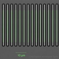
Critical Dimensions
- Line/Space
- VIAs
- Oblong holes
- Overlay
Defect inspection
- Macro defects
- Micro defects
- Particle inspection
- Golden Sample
- Defect detection with AI (deep learning, anomaly detection)
- Feature-based defect classification with neural network
Visual inspection
- KLARF Files
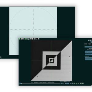
- Visual Inspection with Fine Alignment
- Operator mode (visual inspection)
- Color images
- Depth of field images
- Stitching
- Documentation through comment function
- Digital inking
CONFOVIS WHITEPAPER & CASE STUDIES
Sign up now for our newsletter and gain exclusive access to our whitepaper.
Our newsletter will keep you updated on the latest industry trends, events, product announcements, and exclusive offers. Stay informed and benefit from valuable information that can propel your business forward.

Challenges for the optical inspection of glass & compound semiconductor wafers
DOWNLOAD WHITEPAPER
Full 3D defect and anomaly inspection for inline semiconductor manufacturing
DOWNLOAD WHITEPAPER
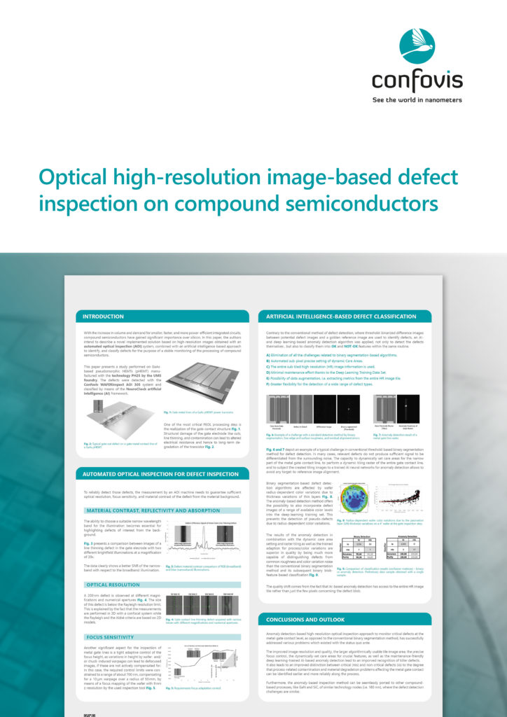
Optical high-resolution image-based defect inspection on compound semiconductors
DOWNLOAD CASE STUDY
Wafer inspection and wafer metrology with Confovis
Confocal measurement of MEMS, 3D Packaging (especially wafer bump measurement), probe mark inspection, LED, roughness, CIS (CMOS image sensor), …
As regards these wafer inspection measurement tasks the reliability of the measurements and the measuring speed are of the essence. 3D measurements with the patented confocal measurement method SIM from Confovis are typically made in two seconds (120 measurement planes with a z-area of 20 µm and an accuracy of < 4nm), with the measurement result being provided irrespective of the surface material to be measured. Even the most difficult combinations of passivation layers and copper can be measured without any problems and prior knowledge.
In the case of micro-electro-mechanical systems (MEMS), it is often necessary to measure multi-dimensional structures which are partly located underneath the surface. With its high degree of accuracy and resolution which comes close to that of an atomic force microscope (AFM), the Confovis WAFERinspect is in a position to measure angles, distances, various dimensions and also roughness.

2D wafer measurements
The autofocus function of the Confovis WAFERinspect uses parts of the confocal beam path, so that the autofocus will work on all surfaces (also on a mirror, to name just one example). The z-axis of the measuring unit, which is there anyway, makes it possible to measure the top and bottom CD in one go, with the results being evaluated with the Cognex software. As a result of an interface between the Confovis and the Cognex software, the absolute distances in a die, the die-to-die shift or also line/space structures smaller than 1 µm can be reliably measured. Redistribution layers (RDLs) in conjunction with the positioning of dies will become measurable during the wafer inspection with Confovis.
Defect Scans
The wafers will be continuously moved and scanned by the metrology tool during the defect scan. The defects thus detected are being cut out and saved during this process together with the associated wafer coordinates.
If macro defects (such as voids, scratches or breakouts) extend over more than one image field, the Confovis WAFERinspect software will automatically put them together. Subsequently, the defects will be rule-based allocated to the trained classes by the neural network in the classificator. This two-step procedure will ensure that also defects hitherto unknown and not trained yet can be detected. Defects without clear allocation will be saved in the class „unsafely classified defects“.
The results of all defects are presented in the Defect Map. In addition to that, they can be issued in the KLARF file format, so that the results can be transmitted via SECS/GEM to the host in compressed form.
Multi-Sensor
Apart from the key component of the Confovis WAFERinspect, i.e. the patented confocal sensor, Confovis pursues the „Best of Class“ strategy. Sensors provided by market-leading third-party suppliers, such as Precitec, LMI or Keyence, can be integrated into the Confovis software without any problems:
- layer thickness sensors
- chromatic confocal and white light interferometry (WLI) sensors
- triangulation sensors
- total thickness variation (TTV) infra-red (IR) sensors
The Confovis measuring system thus proves to be upwardly compatible and allows the user to retrofit it in an inexpensive way, if and when new measuring jobs are pending as part of the wafer inspection (such as another measurement area of the layer thickness).
SECS/GEM and semi standard
The Confovis WAFERinspect can measure and inspect the most diverse types of wafers in combination with a wafer-handling system (equipment front end module, EFEM). Partners for EFEM systems are Mechatronic Systemtechnik and InnoLas Semiconductor. It is possible without retrofitting the hardware to examine the most diverse wafer sizes between 2 and 12 inch on one system. These systems will be available with one or two load ports.
Recipes will be generated via the user interface of the Confovis system and do not require any programming skills. Evaluations made during the wafer inspection just once can be saved as recipe by a mere click and be evaluated with any software, such as MATLAB, Python or by individual Confovis plug-ins. GDS-II coordinates or the Confovis software will be used for the navigation that is teachable with three clicks by a wafer layout. Besides, it is possible to create and load KLARF files.
Wafer Handling
Special edge grip end effectors and chucks, on which the wafer rests exclusively on the edge, are a prerequisite for handling MEMS wafers.
When measuring transparent wafers and wafers with warpage and bow, the system benefits of the Confovis WAFERinspect’s confocal key component in conjunction with the wafer handling system (EFEM) are especially noticeable.
Wafer Inspection with Confovis
The Confovis WAFERinspect metrology tools combine the advantages of defect detection and dimensional measurements.
In doing so, macro and micro defects will be detected, classified and subsequently dimensionally measured by means of a review tool at high speed. The use of a wafer loader that is able to load the most diverse types of wafers (e.g. MEMS, glass, warped, TAIKO, frame etc.) will allow performing the most demanding measurement tasks as part of the automated process control.
MEMS, Micro LED, Mebran, Probe Marks, Bond Pads & Wires, RDL (Redistribution layer), UBM, Silicon, Prime Silicon, Glass, SOI, Sapphire, GaAs, SiC, GaN, InP, GaSb, Ge, LiTaO3, LiNBO3, epitaxial
E5 (Equipment Communication), E10 (RAM), E30 (GEM), E37.1 (HSMS), E39 (Object Services), E94 (Control Job Management), E40 (Process Job Management), E87 (Carrier Management), E90 (Substrate Tracking), E84 (Carrier Handoff Interface)
ARE YOU LOOKING FOR A SOLUTION FOR YOUR APPLICATION?
CONTACT US!