
Confovis
Power semiconductors
The market for components consisting of power semiconductors (e.g. made of silicon carbide [SiC]) is growing, as is the case with the production of battery-powered cars and other applications.
At the same time, the use of SiC wafers presents new challenges for the automated optical power semiconductor inspection of the wafer surfaces. It is one of the biggest challenges for the SiC defect inspection to reliably inspect inhomogeneous surfaces during the process monitoring.
The Confovis WAFERinspect AOI allows a selection of areas for the high-resolution power semiconductor inspection (0.1 µm/pixel) with the help of Care Areas and the distinction of process errors caused by structure variations by means of artificial intelligence. Both feature-based classifiers that are trained by neural networks. Also Deep Learning Methods are available for this purpose.
The constantly increasing requirements concerning the components’ reliability (as is the case with autonomous driving, as an example) make an optical inspection necessary during the early process steps. The aim is to detect defects that have a negative impact on the components’ service life that cannot be identified during an electrical test.
The patented Confovis high-end optics and illumination strategy makes it possible to detect small defects with high resolution in power semiconductors. Irrespective of the surface’s contrast, the Confovis WAFERinspect AOI keeps the structure in focus which is to be inspected. It is therefore possible to use objective lenses with a high numerical aperture (NA), in order to benefit from maximum lateral resolution of light-optical inspection systems.
Why Confovis for the inspection of power semiconductors?
Technologies
Sign up now for our newsletter and gain exclusive access to our whitepaper.
Our newsletter will keep you updated on the latest industry trends, events, product announcements, and exclusive offers. Stay informed and benefit from valuable information that can propel your business forward.
Defect inspection
3D measurements
2D measurements
Critical Dimensions
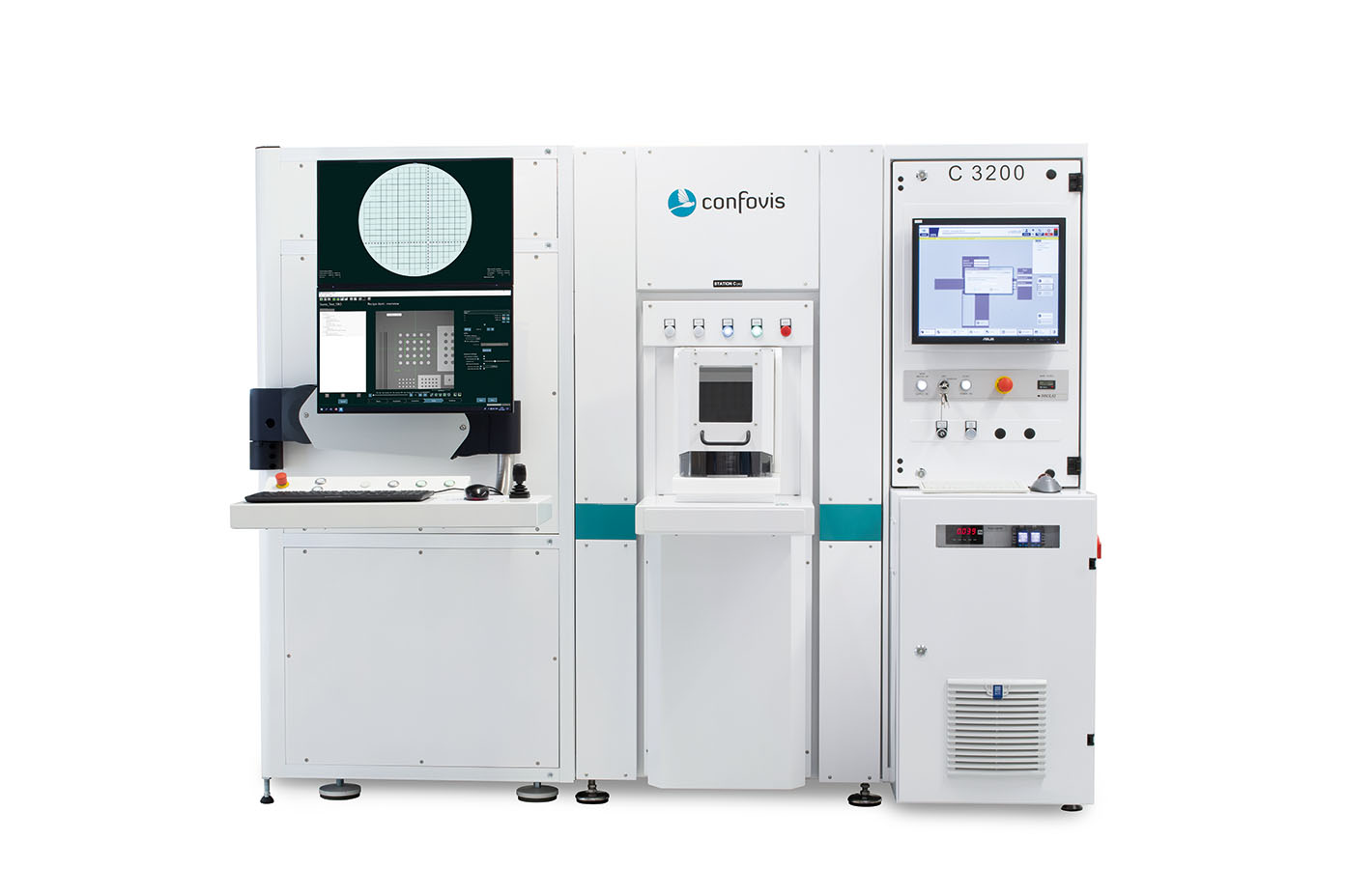
The Confovis WAFERinspect AOI tool combines various inspection jobs on power semiconductors. By combining automated optical inspection (AOI) with metrology, Confovis AOI is able to offer solutions for the defect inspection and classification as well as 3D and 2D measurements (Wafer Level Metrology).
ARE YOU LOOKING FOR A SOLUTION FOR YOUR APPLICATION?
CONTACT US!
Frank Thielert
info@confovis.com
Tel: +49 3641 27 410 – 00