Inline wafer inspection and metrology for VCSEL manufacturing
The laser diode market is growing fast thanks to applications such as facial recognition in entertainment electronics and LiDAR (light detection and ranging) in automotive applications.
Fast and reliable inline quality control of VCSELs manufacturing
VCSEL (vertical-cavity surface-emitting laser) is a type of semiconductor laser diode. Contrary to conventional edge-emitting semiconductor lasers (EEL), VCSELs emit a beam from the top surface. This emission allows them to be tested on-wafer before they are diced into individual devices. Even though the VCSEL production process is more labor and material intensive, the fabrication costs are reduced and the production yield can be better controlled. This requires fast and highly reliable inline quality control of VCSELs manufacturing.
Unlike other automated optical inspection (AOI) systems, the WAFERinspect can perform high precision measurements while continuously scanning the surface of the wafer. This unique feature combines 2D and 3D metrology with defect inspection for a comprehensive analysis of all the process steps in the field of semiconductor manufacturing.
The image correlation algorithm from Confovis allows to find, measure, and fit features such as angles, distances, and radii much faster than any other AOI system.
Use Case: on-the-fly-metrology
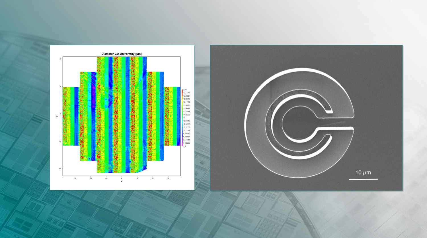
In this use case, we present the on-the-fly metrology performed on 4” silicon wafers. The layout contains 75’000 devices with a top layer consisting of 4 concentric circles. A color-coded map was applied for a graphical representation of the uniformity of the critical dimension of the inner diameter. This is made possible by the speed of the continuous scan of the wafer and the excellent quality of the raw images from which geometry measurements can be processed automatically.


