

To investigate the topography fidelity of optical measurement instruments, a semiconductor calibration standard has been designed and manufactured by Confovis following the guidelines of the German National Metrology Institute.
The device consist of nano-structured concentric circles called circular chirps. They are the first semiconductor calibration samples dedicated to the determination of the transfer function and topography fidelity for AOI tools and 3D optical confocal microscopes.


Automated optical inspection systems are essential tools for all semiconductor manufacturing lines wanting to increase their production yield and quality while reducing costs.
The WAFERinspect systems are state-of-the-art tools for AOI, metrology and defect inspection in the semiconductor industry. They can operate as stand-alone tools or bridge tools in semiconductor fabrication plants. Depending on the type of substrate and measuring tasks, multiple sensor configurations for non-contact, non-destructive measurements are available.
With the increase in volume and demand for smaller, faster, and more power-efficient integrated circuits, compound semiconductors have gained significant importance over silicon.
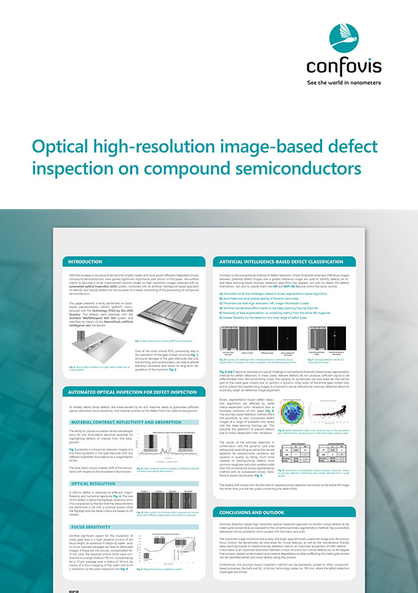
In this case study, the authors intend to describe a novel implemented solution based on high-resolution images obtained with an automated optical inspection (AOI) system, combined with an artificial intelligence-based approach to identify, and classify defects for the purpose of a stable monitoring of the processing of compound semiconductors.

Compound semiconductors are found in a growing range of technology applications. The compound semiconductor market is a multi-billion market which is expected to grow by one order of magnitude within the next decade.
To keep up with the pace and to remain competitive, it is of primary importance for semiconductor manufacturers to increase their yield while reducing costs. Moreover, the constantly increasing requirements concerning components’ reliability make an optical inspection necessary for all critical processing steps.
SIE SUCHEN NACH EINER LÖSUNG FÜR IHRE APPLIKATION?
KONTAKTIEREN SIE UNS!


Sie müssen den Inhalt von reCAPTCHA laden, um das Formular abzuschicken. Bitte beachten Sie, dass dabei Daten mit Drittanbietern ausgetauscht werden.
Mehr InformationenSie müssen den Inhalt von reCAPTCHA laden, um das Formular abzuschicken. Bitte beachten Sie, dass dabei Daten mit Drittanbietern ausgetauscht werden.
Mehr Informationen