
MEMS inspection & MEMS metrology
MEMS inspection & MEMS metrology
MEMS (micro-electro-mechanical systems) are micro-mechanical electronic components that can be either sensors or also actuators. MEMS will count among the electronic megatrends also in the years ahead and find their application in the fields of autonomous driving, 5G, artificial intelligence or microfluidics. The number of MEMS in smartphones and wearables (gravitation sensors, audio and video sensors, fingerprint sensors etc.) is also constantly increasing. MEMS are produced on wafers, the various materials of which include silicon, compound semiconductors, glass as well as epoxy and different metals.
The Confovis WAFERinspect AOI and metrology tools capture these surfaces, irrespective of the materials involved, in 3D and 2D and can thus be used for comprehensive measurement tasks in the field of MEMS inspection and MEMS metrology.
Automated optical MEMS inspection
MEMS achieve a higher degree of reliability than discretely arranged sensors and actuators. This can be explained with the disappearance of connectors, lines and cables on the one hand and with the use of simple physical effects that allow short response times and functional ways, on the other.
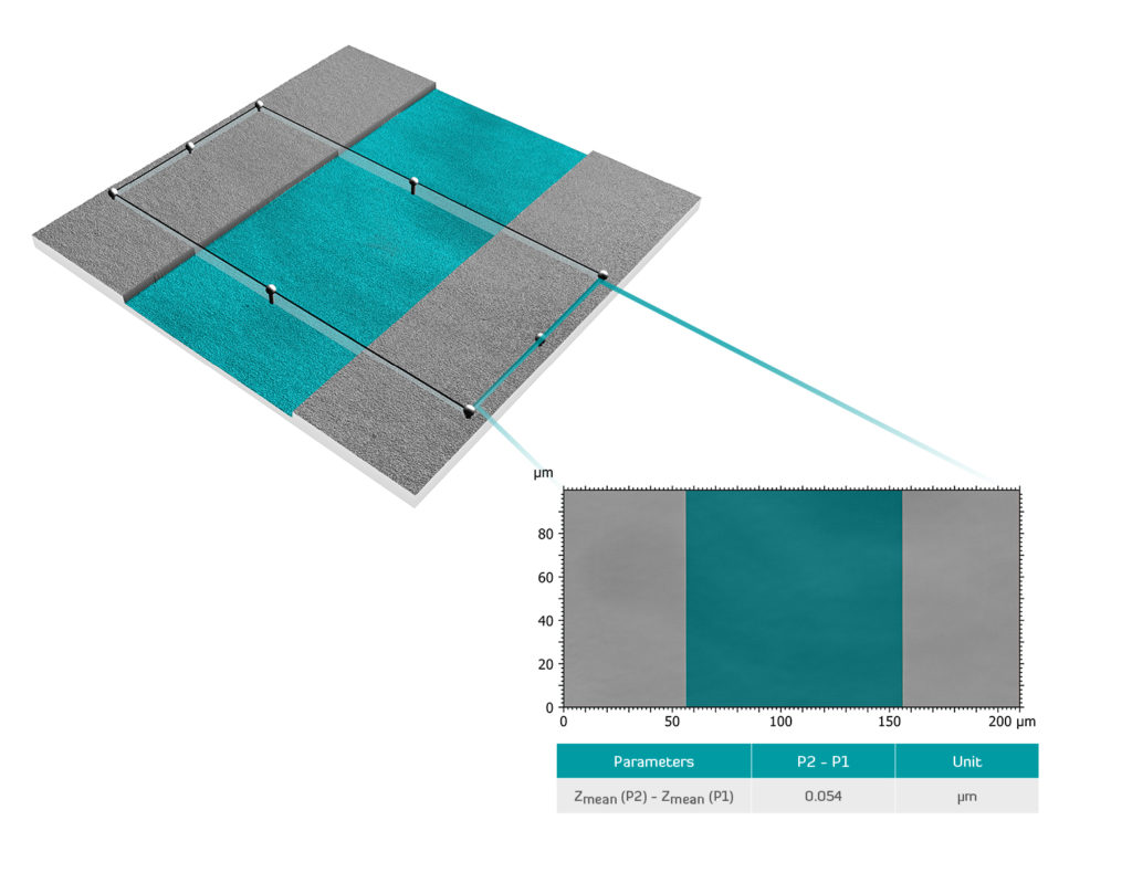
In order to regulate and control production processes, structures must be examined to identify defects (automated optical inspection) and the MEMS must be measured accordingly in 2D or 3D (MEMS metrology). ). Especially in MEMS metrology, Confovis’ patented measurement method Structured Illumination Microscopy from Confovis approaches both the resolution and accuracy of atomic force microscopes (AFM), while the Confovis tool can measure between 100 and 1000 times faster. Another advantage of the Confovis AOI and metrology tools is its 3D measurement that can be operated irrespective of the material concerned, while chromatic confocal sensors and white light interferometers have difficulties in this respect. It is therefore possible to also measure combinations of material, such as gold and epoxy, chromium on glass and polyamides on quartz.
Measurement tasks – MEMS inspection & MEMS metrology
Defect inspection
- Macro defects
- Micro defects
- Particle inspection
- Golden Sample
- Defect detection with AI (deep learning, anomaly detection)
- Feature-based defect classification with neural network
3D measurements
- Independent of materials: silicon, epoxy, glass, chrome, resist, etc.
- Measurements of demanding surfaces without artifacts (no ‘bat wings)
- High speed: 60 confocal frames per second (250 mil. measuring points)
- Film Thickness / Layer Stack
- Topography
- Coplanarity
- Bumps
- Roughness
- Step Height
2D measurements
Critical Dimensions
- Line/Space
- VIAs
- Oblong holes
- Overlay
Visual inspection
- KLARF Files
- Visual Inspection with Fine Alignment
- Operator mode (visual inspection)
- Color images
- Depth of field images
- Stitching
- Documentation through comment function
- Digital inking
Confocal measurement: the advantages of the Confovis measurement method
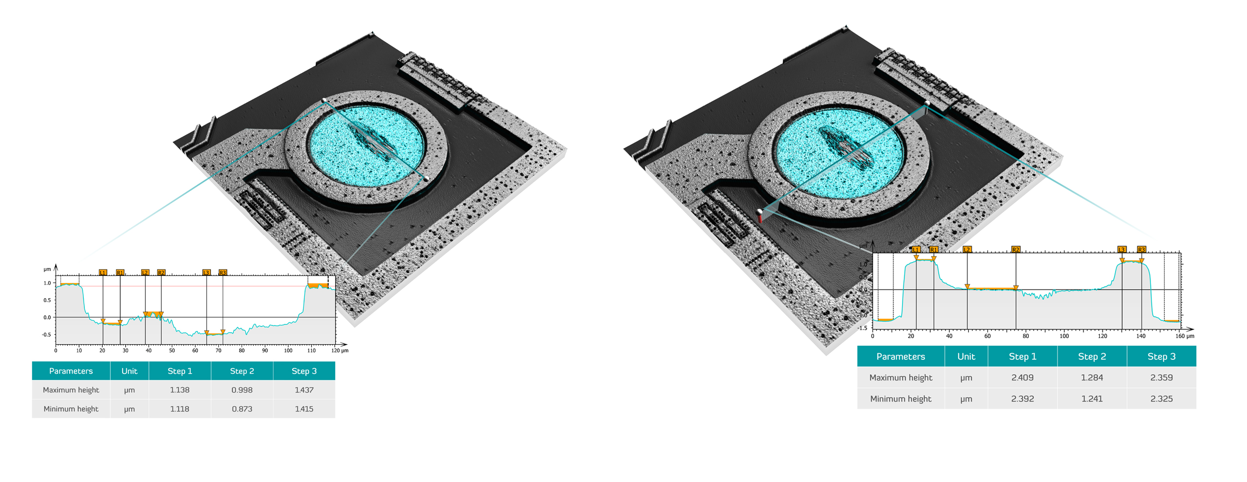
The MEMS inspection especially on wafers with very different structures and a required resolution of under 1 µm is not only challenging but often rather cost-intensive. Thanks to the use of microscope optics, the systems from Confovis can analyze both the entire wafer surface as a large image with distortion correction and also the defects on a die-by-die basis. As an example, cracks in deeper layers of multi-layer MEMS structures can thus be detected by searching the 3D image stack in z-direction for defects.
MEMS inspection system WAFERinspect
A process control instrument is created by integrating the defect detection into the high-resolution MEMS inspection system WAFERinspect AOI, with which defects cannot only be detected but also be measured in 2D and 3D. This will allow immediate conclusions about their emergence. The data will be transmitted to the host via SECS/GEM.
Measurements during the MEMS inspection are carried out with an accuracy of 3 nm and a repeatability of 4 nm @ 3 Sigma (example of a 50 nm step certified by the Physikalisch Technische Bundesanstalt [Germany’s National Metrology Institute]). A precise measurement of angles, distances, radii etc. is also possible. Confovis thus makes a universal and cost-efficient MEMS inspection platform available to its customers.
ARE YOU LOOKING FOR A SOLUTION FOR YOUR APPLICATION?
CONTACT US!