
AOI – Automated optical inspection
confovis ⋯ Solutions ⋯ Semiconductors ⋯ AOI – Automated optical inspection
AOI – Automated optical inspection
The requirements concerning the flexibility of the automated optical inspection (AOI) increase with the trend towards compound semiconductors. The Confovis WAFERinspect AOI system is designed to perform AOI wafer inspection on unstructured and structured wafers. It is not required to manually put in rigid filter limits to detect them, so that, as a result, critical defects will no longer go undetected. Subsequently, the defects will be classified with the help of a neural network.
You are currently viewing a placeholder content from Vimeo. To access the actual content, click the button below. Please note that doing so will share data with third-party providers.
More InformationAOI wafer inspection with Confovis
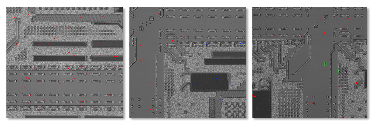
The high-resolution AOI tool WAFERinspect AOI combines defect inspection with a review tool within the same system. It is therefore possible in the case of different structure sizes to inspect the defects with various lenses. In addition to that, the wafers, or the different reticles or dies, will be subdivided into care areas. A stitch image from defects extending over more than one image field can thus be created in this connection, although defects of 0.5 µm will also be detected.
The classificators will be specifically applied in the care area. The automated optical inspection system issues the results of the defect scans as KLARF file or in the system-independent csv format. The user has thus the opportunity to access defects through the wafer map and evaluate them visually. In a second step, the surfaces concerned can be measured with the patented confocal high-speed surface sensor with an accuracy of up to 3nm (wafer inspection). The user-friendly and clearly arranged graphical user interface (GUI) enables users to operate the system intuitively after a short briefing.
Automated optical inspection reduces the inspection costs
The automated optical inspection from Confovis is an advanced, robust and easy method. The real-time image comparison with the golden sample captures defects with a resolution of 1.1 µm and uses the 5x objective with 25 frames per second (fps). Critical areas can be evaluated with a much higher resolution using up to 50x objectives. The advantages of deep learning are hereby used with the help of care areas, in order to find defects on rough and thus optically very different surfaces with a high degree of process reliability.
The option to analyze structures with different light frequencies enables the user to clearly separate defects from the background, depending on material and layer thickness. Positional deviations caused by the hardware will be corrected by the software, so that the Confovis automated optical inspection can also reliably detect defects on wafers after having been diced. Both processes would otherwise involve a high and cost-intensive hardware input for comparable resolution ranges.
AOI wafer inspection in safety-relevant applications
It is more and more often required in safety-relevant fields of the MEMS or microfluidic production (such as in the automotive and aerospace sectors or in the field of DNA sequencing) to inspect not just random samples but the entire range of the dies. In the case 5G technologies, ceramic materials play an important role in the course of implementing this technology. Some of these materials with their demanding dielectric and thermal properties as they are required for 5G are transparent and thus difficult to measure. The AOI system from Confovis is in a position to measure such materials with a vertical accuracy in the nanometer range.
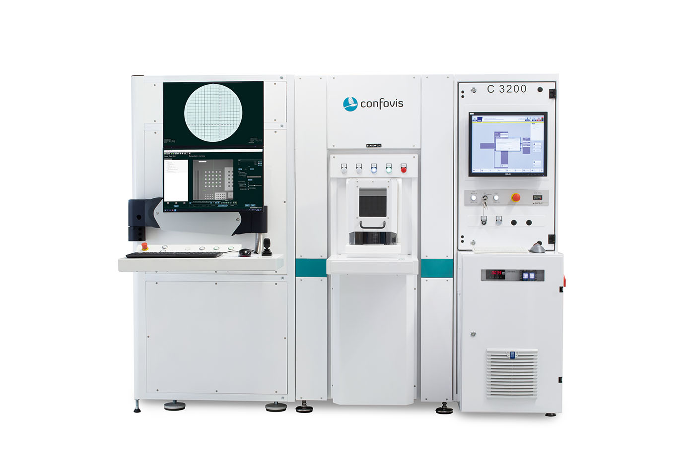
The Confovis AOI and metrology system with its patented, confocal sensor that scans the entire surface (more about the optical measuring technology from Confovis) can be used for capturing 2D image and 3D point clouds for the most diverse positions. The resolution area covers between 0.05 and 2 µm/pixel. The revolutionary handling and imaging concept reduces the measurement time for 300-mm wafers to less than two minutes. The inspection depth and throughput can be optimally adapted to the individual requirements.
The AOI system combines defect inspection, defect review as well as 2D and 3D inspections in just one tool. The Confovis WAFERinspect AOI system can be used for various inspection tasks involving 50 – 300 mm wafers. All typical defect types affecting 2D and 3D structures can thus be detected and classified. The accuracy of the confocal system comes close to the results of the atomic force microscope (AFM) and allows the operator to recognize and monitor critical process changes, which will result in a higher output.
CONFOVIS WHITEPAPER & CASE STUDIES
Sign up now for our newsletter and gain exclusive access to our whitepaper.
Our newsletter will keep you updated on the latest industry trends, events, product announcements, and exclusive offers. Stay informed and benefit from valuable information that can propel your business forward.
Challenges for the optical inspection of glass & compound semiconductor wafers
DOWNLOAD WHITEPAPER
Full 3D defect and anomaly inspection for inline semiconductor manufacturing
DOWNLOAD WHITEPAPER
Optical high-resolution image-based defect inspection on compound semiconductors
DOWNLOAD CASE STUDY
Confovis AOI measurement tasks
Defect inspection
- Macro defects
- Micro defects
- Particle inspection
- Golden Sample
- Defect detection with AI (deep learning, anomaly detection)
- Feature-based defect classification with neural network
3D measurements
- Independent of materials: silicon, epoxy, glass, chrome, resist, etc.
- Measurements of demanding surfaces without artifacts (no ‘bat wings’)
- High speed: 60 confocal frames per second (250 mil. measuring points/s)
- Film Thickness / Layer Stack
- Topography
- Coplanarity
- Bumps
- Roughness
- Step Height
2D measurements
Critical Dimensions
- Line/Space
- VIAs
- Oblong holes
- Overlay
AOI wafer inspection applications
- MEMS
- Micro LED
- 5G ceramic surfaces
- glass wafer
- sapphire
- RDL (redistribution layer)
- laser diodes
- epitaxial layers (GaN on SiC)
- UBM (under bump metallization)
- GaAs
- SiC
- Ge
- LiTaO3
- LiNBO3
- SOI
- GaN
- InP
ARE YOU LOOKING FOR A SOLUTION FOR YOUR APPLICATION?
CONTACT US!