
Confovis
Full 3D defect and anomaly inspection for inline semiconductor manufacturing.
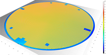
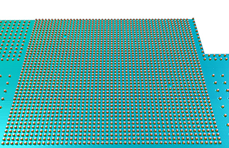
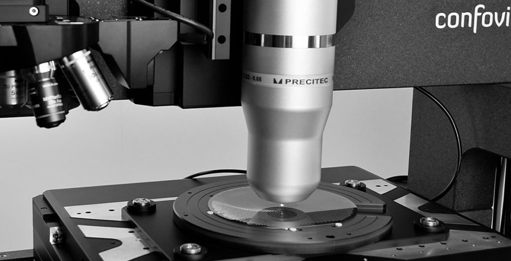
The WAFERinspect AOI Dual is an automated optical inspection (AOI) tool with two high-end sensors for semiconductor manufacturing inspection. The two sensors allow for a two-path approach inspection of wafers up to 300 mm. It is specifically designed for the inspection of lenses and bumps in LiDAR and advanced packaging applications. First, the whole wafer is scanned within minutes to identify defects. Then structure in question are analysed to nm accuracy with the ConfoCam module.
You are currently viewing a placeholder content from Vimeo. To access the actual content, click the button below. Please note that doing so will share data with third-party providers.
More InformationThe WAFERinspect AOI Dual system can perform a full 3D scan of a 300 mm wafer within 2 to 3 minutes. This allows a fast 3D defect inspection. It is of particular interest for micro-lenses and bumps in LiDAR and Advanced Packaging for example.
The availability of the two adjacent sensors allows for a two-path approach:
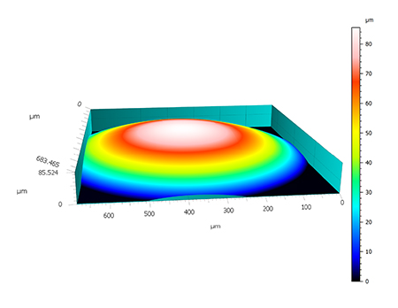
Hence, in a second path, the structures in question can be analysed to single nm accuracy with the Confovis patented optical measurement method.
Structure heights ranging from 50 µm to few mm can be seamlessly measured with the 1200 points white light sensor can cope with it.
Whether it is deformations of micro-lenses for LiDAR or height distributions of bumps in advanced packaging, the AOI Dual system can carry out a 100% 3D defect inspection on big data up to 1 TB/wafer.
The artificial intelligence (AI) capability of Confovis in anomaly detection allows to detect unknown defects.
Additionally, a comparison between the actual shape of the structures and a target (golden sample) is possible.
WAFERInspect AOI Dual: Applications
Sign up now for our newsletter and gain exclusive access to our whitepaper.
Our newsletter will keep you updated on the latest industry trends, events, product announcements, and exclusive offers. Stay informed and benefit from valuable information that can propel your business forward.

ARE YOU LOOKING FOR A SOLUTION FOR YOUR APPLICATION?
CONTACT US!
Frank Thielert
info@confovis.com
Tel: +49 3641 27 410 – 00