
Confovis
Wafer Bump Inspection
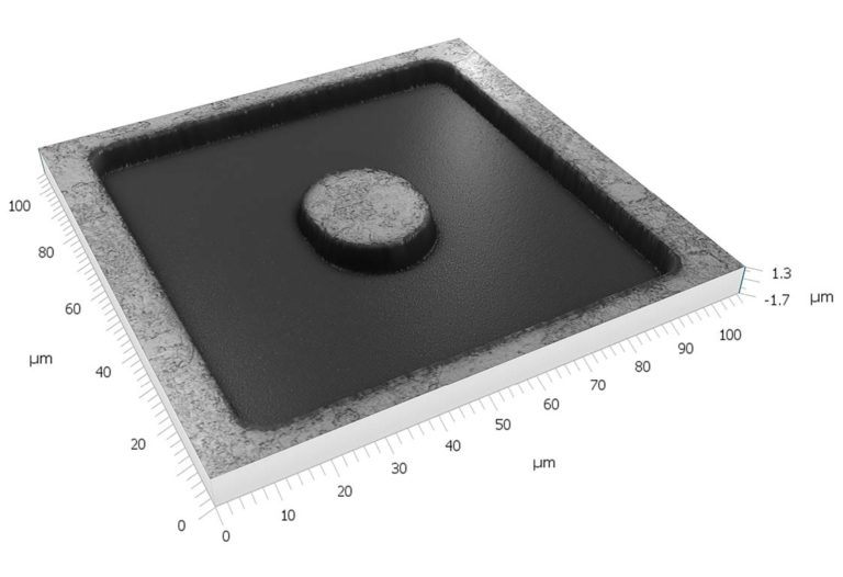
The patented Confovis measurement method is technology leader, where the resolution of bumps (wafer bump inspection) and copper pillars (copper pillar inspection) between 2 µm and 100 µm is concerned. Irrespective of the material involved, not only the height of the bumps but also their shape and surface can be measured (wafer bump metrology).
Based on this technology, the Confovis WAFERinspect AOI Tool has been extended by a high-speed chromatic-confocal line sensor. Customers therefore have the opportunity to completely inspect wafers and panels with millions of bumps in a very short time (wafer bump inspection). It is possible at any time to resort to the Confovis measurement result as gold standard, in order to algorithmically reduce the process-related edge effects of the chromatic-confocal inspection.
It is not required to calibrate the Confovis measurement – irrespective of the material involved and of the ambient surface. The patented structured illumination microscopy (SIM) will ensure an accuracy of < 9 nm @ 3 sigma in the case of structure heights of 4 µm.
A 100%-wafer bump inspection is unavoidable, in order to ensure the reliability rates required for stacked devices in the future. Apart from dimensional measurements, the AOI systems from Confovis offer a wide range of bump inspection and metrology solutions in this respect.
The inspection of bumps and copper pillars includes the detection of missing, bridged and deformed bumps. Another inspection category offered by our systems is the detection of surface defects (such as foreign particles) on a bumped wafer.
Why Confovis for wafer bump inspection and copper pillar inspection??
Wafer bump inspection technologies
Sign up now for our newsletter and gain exclusive access to our whitepaper.
Our newsletter will keep you updated on the latest industry trends, events, product announcements, and exclusive offers. Stay informed and benefit from valuable information that can propel your business forward.

Defect inspection
3D measurements
2D measurements
Critical Dimensions
The Confovis WAFERinspect AOI tool combines various inspection jobs on bump inspection. By combining automated optical inspection (AOI) with metrology, Confovis AOI is able to offer solutions for the defect inspection and classification as well as 3D and 2D measurements (Wafer Level Metrology).
ARE YOU LOOKING FOR A SOLUTION FOR YOUR APPLICATION?
CONTACT US!
Frank Thielert
info@confovis.com
Tel: +49 3641 27 410 – 00