WAFERinspect AOI
Combined automated optical inspection and metrology for serial inspection and measuring tasks
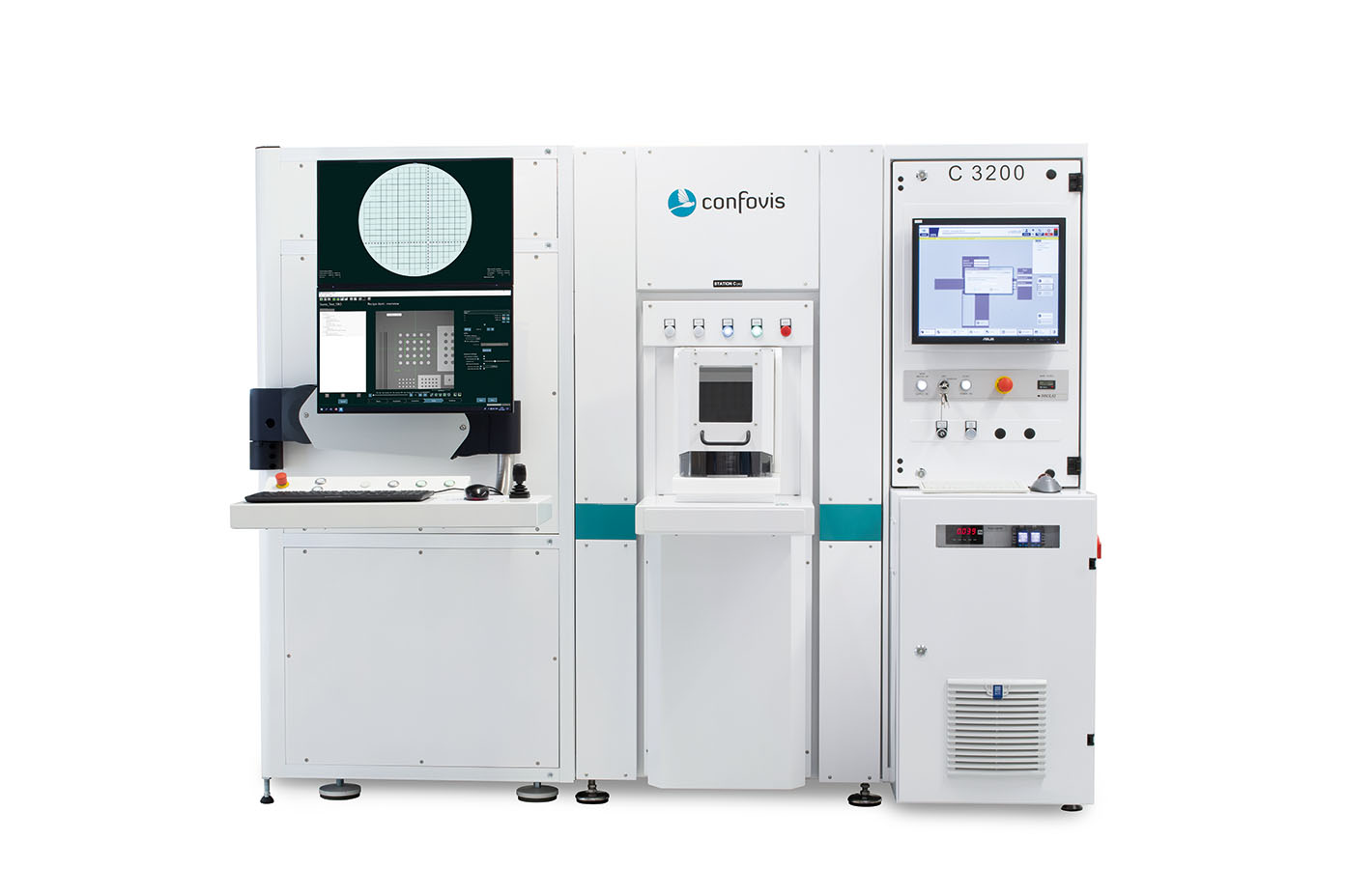
- A single system for various inspection tasks: automated optical inspection & metrology
- Flexibility: rapid adaptation of the system to new requirements in the field of defect inspection
- "Swiss Army knife": automated solutions for 2D and 3D measurements, SECS/GEM, various handling solutions for MEMS, glass, warped, thin or Taiko wafers
- High accuracy and repeatabilities when performing 2D and 3D measuring tasks
WAFERinspect AOI
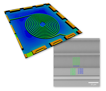
The Confovis WAFERinspect AOI system combines the most diverse inspection tasks involving structured and unstructured wafers in just one system. By combining automatic optical inspection (AOI) and metrology the Confovis WAFERinspect AOI offers individual solutions for defect inspection and classification as well as for 3D and 2D measurements (wafer level metrology) for MEMS, advanced packaging, RDL, bumps etc.

Mit dem Laden des Videos akzeptieren Sie die Datenschutzerklärung von Vimeo.
Mehr erfahren
Defect Inspection

3D and 2D measurements

Software
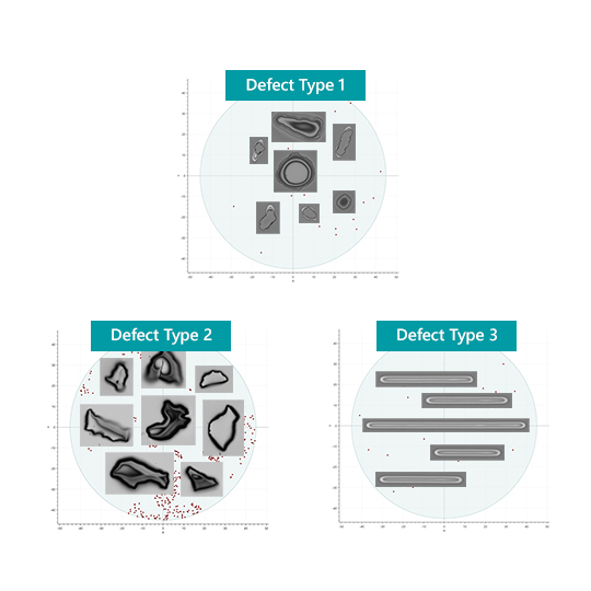
The Wafer Inspect software from Confovis ensures simple handling for the user by combining easy with professional modes, thus offering a maximum of assessment flexibility by way of „geometry measurements“. Formulas can be created within less than five minutes. Defects will be detected and assessed with the fully integrated and adaptable software from our partner NeuroCheck.
WAFERinspect AOI applications
- MEMS
- Micro LED
- 5G ceramic surfaces
- glass wafer
- sapphire
- RDL (redistribution layer)
- laser diodes
- epitaxial layers (GaN on SiC)
- UBM (under bump metallization)
- GaAs
- SiC
- Ge
- LiTaO3
- LiNBO3
- SOI
- GaN
- InP
WAFERinspect AOI – measurement tasks
Defect inspection
- Macro defects
- Micro defects
- Particle Inspection
- Golden Sample
- Defect detection with AI (deep learning, anomaly detection)
- Feature-based defect classification with neural network
3D measurements
- Independent of materials (silicon, epoxy, glass, chrome, resist, etc.)
- Measurements of demanding surfaces without artifacts (no ‘bat wings’)
- High speed: 60 confocal frames per second (251 million measuring points per second)
2D measurements
Critical Dimensions
- Line/Space
- VIAs
- Oblong holes
- Overlay
CONFOVIS WHITEPAPER
Sign up now for our newsletter and gain exclusive access to our whitepaper.
Our newsletter will keep you updated on the latest industry trends, events, product announcements, and exclusive offers. Stay informed and benefit from valuable information that can propel your business forward.
WAFERinspect AOI–
technical Highlights
- Defect inspection and review in one tool
- Flexibility in the field of defect inspection: The inspection can be speedily adapted to any new tasks by way of artificial intelligence
- No defect teaching required before the actual defect scanning process
- Comprehensive 2D and 3D measurements of the most diverse structures (such as roughness, step heights, slopes, bumps, saw cuts, flatness, coplanarity, TSVs,…) and surfaces (silicon, epoxy, glass, chromium, …)
- Very high accuracy and repeatability
- Wafers ranging between 2 and 12 inches (SEMI, JEIDA, non-standard…)
- Substrate handling: wafers, frame, warped, thin, waffle pack, porous
- Handling options for highly warped wafers and Taiko handling options
- Flexible platform for further sensor integration
- Online und offline review capability
Frank Thielert
info@confovis.com
Tel: +49 3641 27 410 – 00
- Fast and with nanometer precision
- Flexibel
- High level of automation