
Confovis
Detailed 3D/2D measurements for the process control in the field of semiconductor production
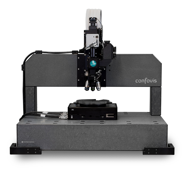
The WAFERinspect metrology tool from Confovis combines 3D and 2D measurements for a comprehensive analysis of the most diverse process steps in the field of semiconductor production. The confocal 3D measurements are carried out irrespective of the surface material to be measured with an accuracy of <4nm. Line/space, VIAs and overlay structures can also be measured in 2D with a high degree of accuracy (Wafer Inspection). Confovis WAFERinspect is available both as fully automated system with SECS/GEM and EFEM application and as laboratory equipment.
The Confovis WAFERinspect metrology system allows measurements of line/space structures smaller than 1µm, of diameters, distances, overlays etc. The 2D measurements are carried out die-based, while the measurement recipes can always be individually created and easily as well as speedily adapted to changing processes. The object recognition is implemented on the basis of the Cognex image processing software, so that the object coordinates can be used for various calculations and be combined ad lib. The focus layer will be found on all surfaces with high process reliability by the confocal auto-focus, which makes it possible to carry out line/space measurements with top and bottom fit even with higher resist thicknesses. The flexibility of the 2D measurements can be extended by 3D measurements.
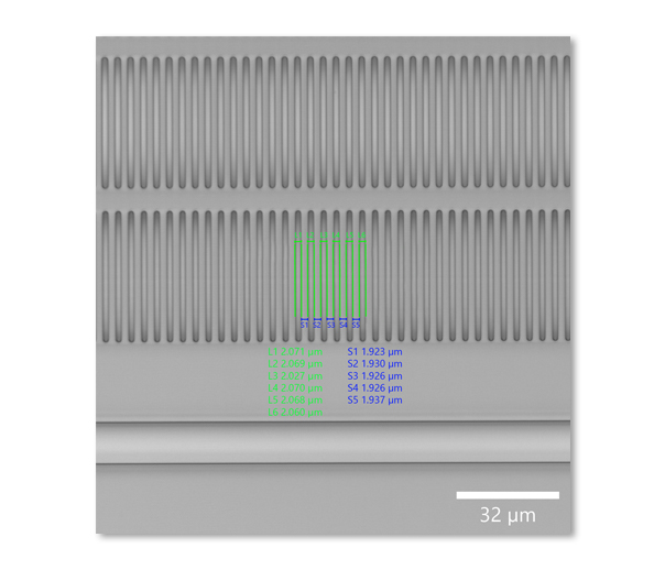
In the case of certain structures (such as steps, bumps, bond pads, probe marks, …) a 3D measurement is required for more detailed analyses, apart from the 2D measurement. All 3D structures can be measured in their entirety with the measurement technology Structured Illumination Microscopy that has been patented by Confovis. The measurements are made within two seconds, so that, as an example, the position of a step can be found by a function fit to the 3D data and the distance to the next step can be established with Cognex. The coordinates thus found will increase the accuracy of the 2D measurement linked with it (e.g. in the case of line/space). In addition to that, also underetchings can be made visible by multi-signal analyses at the transparent level stack.
The WAFERinspect software from Confovis offers easy handling and a maximum of flexibility by linking easy modes and advanced modes. Recipes can be created in less than five minutes. Typical measurement jobs, such as line/space or the establishment of diameters, can be taught with three clicks (easy mode). The image evaluation of the measurements is based on the Cognex image processing software and all features of Cognex can be used by including the template function. The objects and coordinates can be used for calculations with all mathematical expressions and thus for presenting even complex measuring tasks.
Sign up now for our newsletter and gain exclusive access to our whitepaper.
Our newsletter will keep you updated on the latest industry trends, events, product announcements, and exclusive offers. Stay informed and benefit from valuable information that can propel your business forward.

Defect inspection
3D measurements
2D measurements
Critical Dimensions
Visual inspection

ARE YOU LOOKING FOR A SOLUTION FOR YOUR APPLICATION?
CONTACT US!
Sebastian Schenk
info@confovis.com
Tel: +49 3641 27 410 – 00