Optical high-resolution image-based defect inspection on compound semiconductors
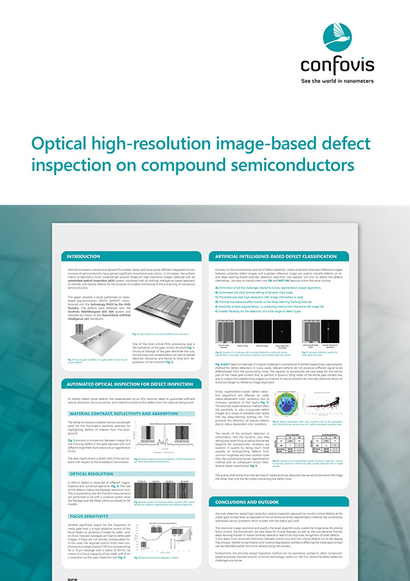
With the increase in volume and demand for smaller, faster, and more power-efficient integrated circuits, compound semiconductors have gained significant importance over silicon. This case study describes a novel implemented solution based on high-resolution images obtained with an automated optical inspection (AOI) system, combined with an artificial intelligence-based approach to identify, and classify defects for the purpose of a stable monitoring of the processing of compound semiconductors.


Case Study Download
Your subscription could not be saved. Please try again.
Your subscription has been successful.
SIE SUCHEN NACH EINER LÖSUNG FÜR IHRE APPLIKATION?
KONTAKTIEREN SIE UNS!

