LiDAR Inspection
The semiconductor market linked to autonomous vehicles has more than doubled from 2015 to 2022 and it is expected to continue to grow over the next years representing one of the highest growth segments in the semiconductor industry.
Advanced driver assistance systems (ADAS) and fully autonomous vehicles require the automation of various aspects of the driving process like parking assistance, lane positioning, and collision avoidance. These technologies use multiple sensors such as LIDAR (Light detection and ranging), radar, and image sensors. LIDAR has already been successfully applied in many fields of operation such as robotics navigation and land surveying. They are now among the most promising technologies for ADAS.
Quality management of MEMS-based LiDARS
The emergence of micro-optical MEMS and micro-mirrors is providing a promising solution to low-cost, reliable, and highly integrable LiDAR systems. MEMS-based LiDARs are trending right now towards ADAS and fully autonomous vehicles. Their manufacturing on wafers makes them highly scalable with thousands of identical components produced in a cost-efficient manner.
The quality management of such microsystems is challenging. Thin layers must be inspected on the same substrate as micro-lenses or micro-mirrors with thicknesses that can reach from micrometer to millimeter. The micro-mirrors used in MEMS LiDARs are photonics microsystems. They are fabricated on large diameter silicon wafers which require reliable inline test equipment for non-destructive inspection to assure quality in product development and manufacturing.
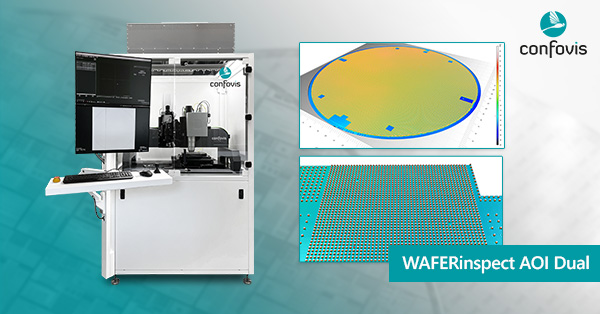
The WAFERInspect AOI Dual tool for LiDAR inspection
The WAFERinspect AOI Dual system is of particular interest for MEMS in general, and for LiDARs specifically, as it can cope with topographies ranging from few nm to mm on the same wafer. Thanks to the two high-end sensors equipping this new automatic optical inspection system can perform a full 3D scan of wafers up to 300 mm within to 2 to 3 minutes followed by a 100% 3D defect and anomaly inspection with single nm accuracy.