
Confovis
Finding & classifying wafer defects & impurities with high process reliability
Defects need to be identified on (MEMS-)wafers, microfluidic wafers etc. (defect inspection), in order to monitor and control production processes more effectively. Apart from the mere existence of a defect, its impact on the subsequent process or on the end product’s functionality is crucial. It is for these reasons that the properties of defects must eventually be analyzed and divided in different classes, in which case the topological properties in 3D are, among other things, decisive (wafer inspection). By integrating defect inspection & classification into the high-resolution WAFERinspect measuring and defect inspection systems, Confovis offers a process control instrument, with which defects can be identified as well as classified with the help of a neural network. Also, all structures can be measured in 2D and 3D.
AOI defect inspection with Confovis benefits from the excellent optical quality of the defect inspection tool WAFERinspect AOI that makes it possible, as an example, to create a stitched image from larger defects, such as delamination lines. Both the illumination homogeneity and the distortion of the lenses are then corrected in such a way that a defect image is made available to the users.
Besides, different light frequencies allow for a high-contrast presentation of the most diverse materials. Depending on the objective of the analysis, transparent passivation layers can be deliberately put into the focus by the automatic focus that is integrated into the system or can be faded out.
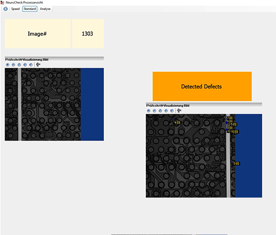
The defect detection works either in the classic way, i.e. via Blob Detection according to the golden sample method, or by way of artificial intelligence according to the deep learning method. The Confovis WAFERinspect detects defects of any kind without prior training, with the defects being classified in a process after the detection. Either filters or a neural network are available for the rule-based analysis. It is an advantage for the user that no defects will remain undetected, even if the defect classes are unknown.
Sign up now for our newsletter and gain exclusive access to our whitepaper.
Our newsletter will keep you updated on the latest industry trends, events, product announcements, and exclusive offers. Stay informed and benefit from valuable information that can propel your business forward.

The wafer defect inspection especially on wafers with very different structures and required resolutions of up to under 0.5 µm is rather challenging and, in most cases, cost intensive. The defect inspection tools from Confovis use high-quality microscope optics, so that image field and resolution can be optimally adapted to the measuring task concerned. Even defects with a lateral expansion of 0.5 µm can be found and classified with high process reliability. The training of the defect inspection can be accomplished by the users in a few easy steps and adapted to the relevant needs at any time.
Confovis is able to continuously scan the entire structured or unstructured wafer surface. Either the entire surface or areas thereof determined beforehand (so-called care areas) will then be assessed based on a golden sample comparison or by way of artificial intelligence (AI). The defects will be fully automatically sorted into classes by the software on the basis of classifiers after a one-off teach-in or sorting procedure (defect classification). A great strength here is the application of artificial intelligence, so that defining rigid threshold values can be dispensed with and the defect inspection can be adapted to changing processes at any time. Not only will the defects be assessed and classified by using the threshold values but also especially on the basis of neural networks. In this way, the classifiers make it possible to train and categorize newly emerging defects. The automated defect detection benefits greatly from the high transmission speed with real-time hardware control and calculation processes on FPGA technology.
Selected parts of the structure (e.g. reticles, dies or bump patterns) can be fully measured in 3D within seconds during the set-up process or when the need arises. The users will thus gain knowledge and insights from the Confovis WAFERinspect AOI as a full-feature process control instrument. As an example, hair cracks in multilayer processes, caused by tension in surfaces, are often so weak in contrast or small that light-optical measuring methods reach their limits. Cracks can now be detected on the basis of the changing surface topography by using the 3D measurement option of the confocal Confovis sensor with its nanometer precision.
Probe marks place particular demands on the wafer defect inspection: The combination of 2D defect inspection and high-precision 3D measurement allows for a quantitative analysis of any changes affecting the pin prints, thus facilitating an automated combination of defect inspection and 3D measurement of the critical probe marks, in order to readjust the probing process as early as possible.
The WAFERinspect AOI system from Confovis provides the customer with a universal and cost-effective metrology platform that integrates defect detection and 2D/3D measurements into one system. The data are transmitted to the host via SECS/GEM. The measurements are made with an accuracy of 3 nm and with a repeatability of 4 nm @ 3 Sigma (example of a 50 nm step certified by the Physikalisch Technische Bundesanstalt [National Metrology Institute of Germany]). Angles, distances radii etc. can also be measured precisely.
ARE YOU LOOKING FOR A SOLUTION FOR YOUR APPLICATION?
CONTACT US!